Project Researcher: Chris Williamson
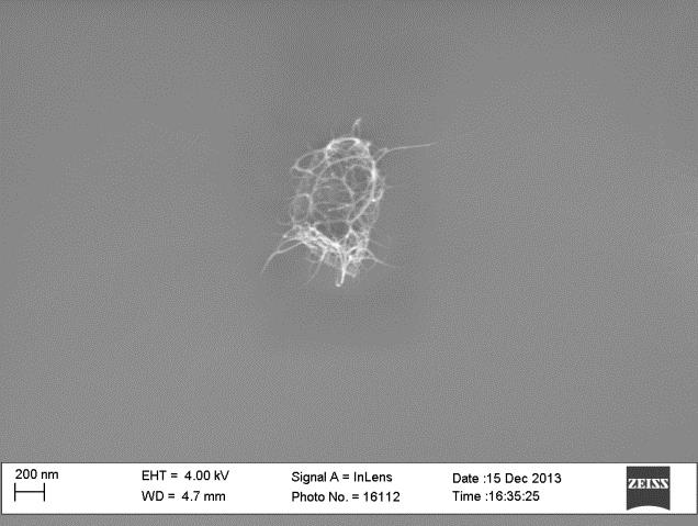
The research in this project has been developing a novel method if ion beam patterning in order to position carbon nanotubes (CNTs) in a pre-determined location. The CNTs were initially grown using an ion catalyst but the resultant structures were very fine and relied on Van der Waals forces to maintain their upright stance. Although a field of CNTs and patterning of the catalyst were achieved independently, combining the techniques together in an attempt to achieve freestanding aligned CNTs resulted in a lack of vertical alignment as shown in Figure 1. Figure 2 shows an attempt at massive growth on a silicon substrate with a nickel catalyst.
It was determined that the lack of alignment could be due to insufficient structural stability in the CNT, a lack of sufficient electric field or insufficient etching of the catalyst to form nanoparticles.
Read more about this stage of the project in the Mid-Term Report 2014.
In order to have a degree of control of field emission, it was determined that a conductive underlayer to the catalyst was required which would enable a circuit to be patterned prior to CNT growth. Figure 3 demonstrates growth using titanium which is whispy and it was not possible to improve on this result. The reason for this is that the nickel catalyst layer diffuses into the Ti underlayer and the resultant catalyst sites are very small. Similar problems were found with all metals. It was found that an oxide based underlayer yields good growth (Figure 4) and when the layer is thinner than 4nm electrons can tunnel through to a metal layer below. Unfortunately around the same threshold, the oxide layer is too thin to improve growth and diffusion of the catalyst into the metal underlayer is dominant. The solution to the problem was to use indium tin oxide (ITO) as an underlayer (Figure 5) which is conductive and also an oxide. A 10nm ITO layer with 6nm Ni catalyst layer yielded uniform vertically aligned CNTs on a conductive material which is an ideal platform to build a field emission circuit onto.
Read more about this project in the Centre’s 2014-2015 annual report.
This research project is being undertaken at the University of Cambridge, supervised by Prof Daping Chu.


